Effect of Parasitic RLC Parameters in GSM Band Amplifier
Introduction
This application demonstrates effect of parasitic RLC parameters on forward transmission coefficient (S21) in GSM band Signal Amplifier. Simulations are performed in EMCoS PCB VLab and EMC Studio. Parasitic effects are considered separately for all conductive traces along main signal path. This realistic model is compared to ideal case when wires only connect functional elements in equivalent circuit and do not affect design performance.
Measurement Setup
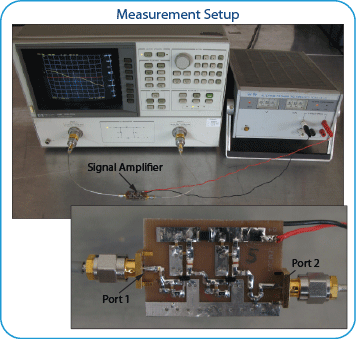
Measurement setup and equivalent circuit for Signal Amplifier (GSM Band) are shown below.
Measurements were performed in EMCoS laboratory.
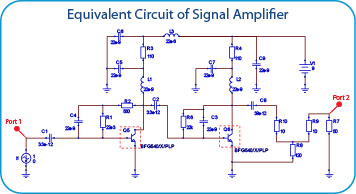
BFG540/X/PLP transistors included in Amplifier circuit are modeled in System Simulation model as Touchstone devices defined from manufacturer’s s-parameters datasheet (as *.snp files).
Simulation Model Description
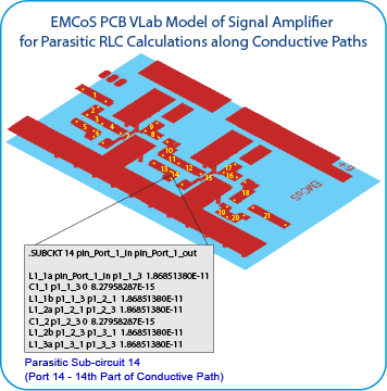
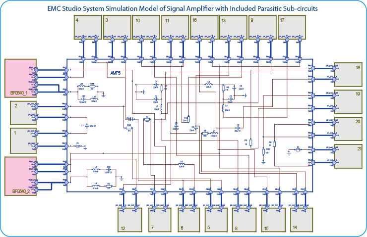
Calculation of parasitic RLC elements and generation of equivalent circuit are performed in EMCoS PCB VLab environment. PCB model of signal amplifier is obtained from ODB++ format and parasitic L and C coefficients are calculated for each conductive path. Each pair of ports on the figure represents a part of conductive path which is then translated to parasitic sub-circuit. Totally 21 parasitic sub-circuits are obtained for complete conductive path. Generated parasitic circuits are integrated in amplifier equivalent model for system simulation analysis in EMC Studio.
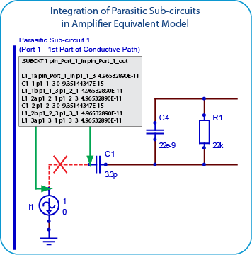
System simulation model for Signal Amplifier with included parasitic sub-circuits is shown below (devices colored in grey represent parasitic sub-circuits and red color devices – transistor models defined from manufacturer’s s-parameters datasheet):
Results
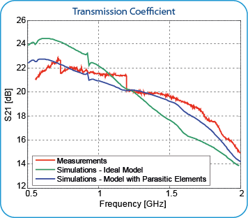
Simulation results for both ideal and realistic models of Signal Amplifier are compared to measurements. Realistic model of Signal Amplifier with parasitic effects gives better agreement with measurements.
Conclusions
- Rapid RLC solver included into EMCoS PCB VLab provides parasitic RLC extraction and generation of equivalent circuit for analysis of parasitic effects on PCB
- Generated parasitic circuit can be used further in EMC Studio system simulation analysis
- Realistic model of amplifier with parasitic sub-circuits gives better agreement with measurements then ideal model
